EUV Lithografie explained by ASML (uitgesteld, i.v.m. coronavirus)
EUV Lithografy
What is EUV Lithografy, what are the possibilities and challenges and are the expected milestones reached so far?
On April 23, it will be explained during a visit to the Experience Centre of ASML
some recent information can be found here :
https://www.ed.nl/asml/tsmc-meldt-levering-van-eerste-euv-chips-voor-consumenten~a476725d/
https://www.anandtech.com/show/14992/euv-demand-up-at-asml
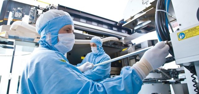
Using a wavelength of just 13.5 nanometers (nearly x-ray level), our EUV technology can do big things on a tiny scale.
Developed over 20 years of sustained R&D, our machines are now gearing up to power the next generation of integrated circuits during at least the next decade.
Lithography that shapes the future. Providing highest-resolution lithography in high-volume manufacturing, ASML’s EUV machines are pushing Moore’s Law forward.
Speaker
During this visit to ASML dr.ir. Patrick W.H. de Jager ASML sr. director New Business will first give a presentation on the development, progress of EUV and a overview about the new products.
There will be ample time to ask questions for further explanation.
After the presentation we are invited to visit the ASML Experience Center where many components of the EUV machines are on display and will be explained.
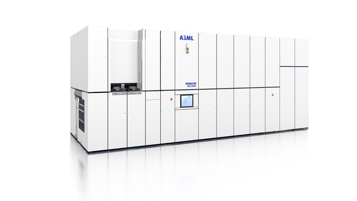
The TWINSCAN NXE:3400C is ASML’s latest-generation lithography system, supporting EUV volume production at the 7 and 5 nm nodes.
Technology
More about the ASML Technology see Big steps in tiny patterns
Name and contact for Information
Dr.Ir. Eric Persoon Member of the Royal Netherlands Engineering Society, department Electrical
Engineering, Team EnergyNL2050 E-mail eric,persoon@upcmail.nl
Programma |
|
|---|---|
| - uur | Arrival and reception Visitors Building 7 |
| - uur | EUV Lithografy by dr.ir. Patrick W.H. de Jager ASML sr. director New Business |
| - uur | Visit Experience Centre ASML |
| - uur | Networking with drinks |