Company visit ASML with lecture & Demo.
Short report on the visit of KIVI-EL to ASML on October 12, 2017:
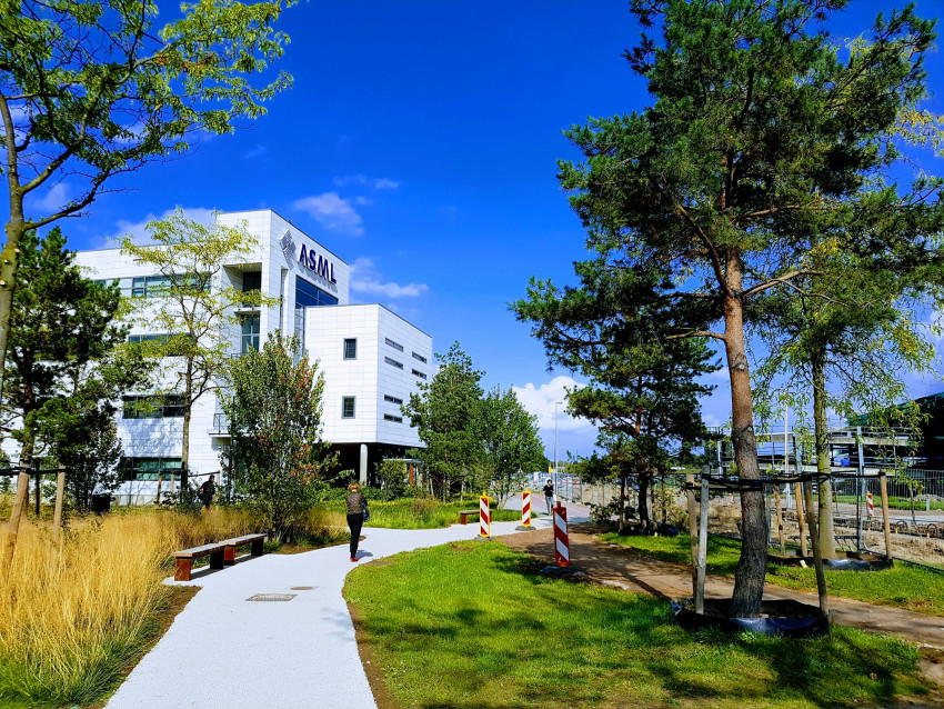
ASML Veldhoven site
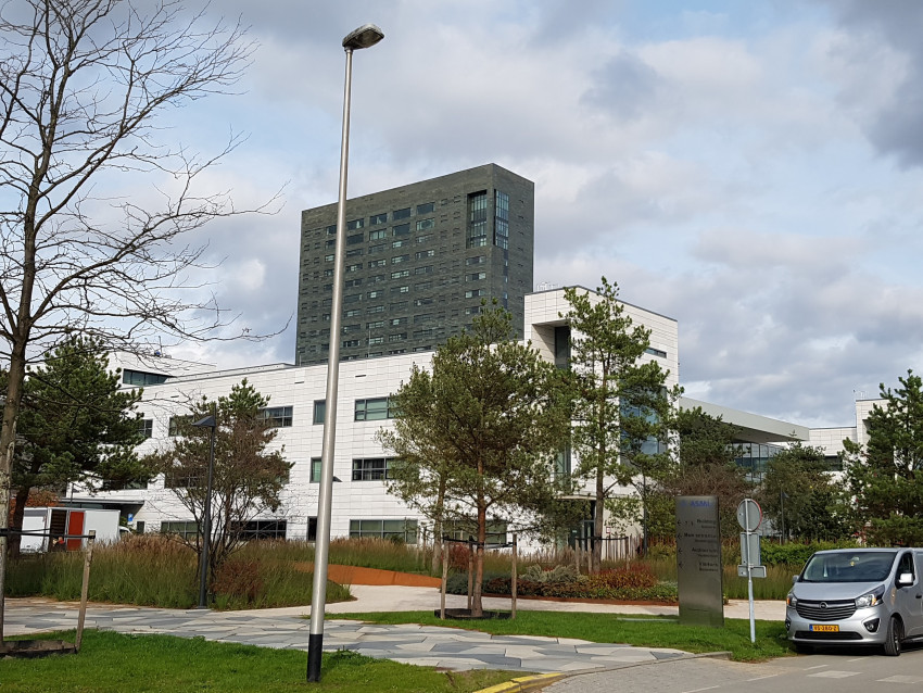
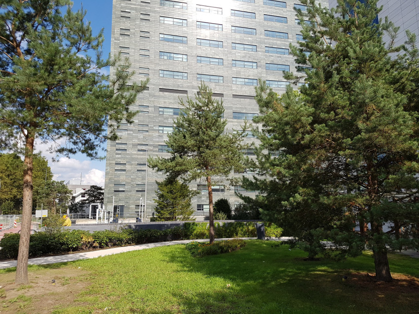
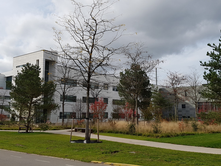
Indeed an impressive site in Veldhoven close to the highway towards Antwerp. The high-rise central building and next to it all the labs and office buildings. And next to those the cleanroom production facilities.
We were hosted by Maarten Hoeks (Manager Electrical Architecture Group) and Jeroen van Duivenbode (Competence Leader Power and High Voltage Electronics and Fellow at TUe Department of Electrical Engineering).
The site houses about 1/3 of the ASML employees. Total number is 17.000 (fte) and at the Veldhoven site 6.500 are located. After smooth entry procedures we embarked on a coffee in the huge canteen.
Moore’s law
The topic our visit was: Power Electronics keeps ASML systems going.
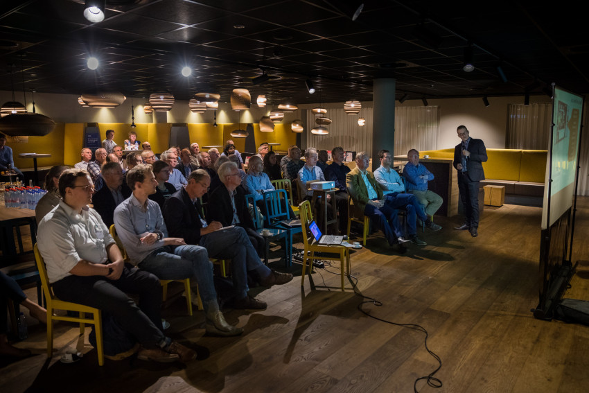
Maarten gave a nice view on what ASML is all about: see to it that the industry can follow Moore’s law in an economical way.
So they went all the way from the first systems in 1984 (PAS2000) to the TwinScan NXE using an EUV light source in 2016. For EUV the lenses have been replaced by mirrors and the system operates in vacuum.
Next to the Scanner hardware more and more business of ASML is created by supporting services related to optimizing the wafer-quality.
Key technical issues are:
-
Stage accuracy (nm accuracy)
-
Overlay (nm accuracy)
-
Alignment (nm accuracy)
-
Throughput (wafers/hour, reliability)
High requirements should be met to enable reliable operation of the scanners to produce multilayer wafers. In these requirements power amplifiers and proper (feed forward) control play a major role.
Power Electronics is vital to the success of ASML is the summary of Maarten.
Power and High Voltage Electronics
High Power
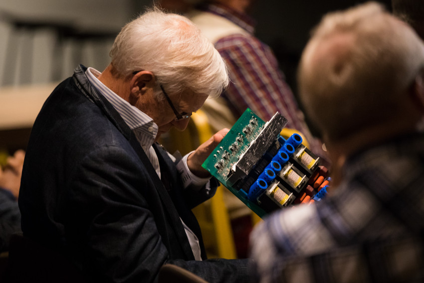
Because of the vacuum inside EUV scanners new technology was needed to move and lift the wafer stage. A combination of coils and permanent magnets enables lifting the stage and moving the stages.
A typical number is the following: let’s project the 300 mm wafer on the Netherlands with a radius of around 300 km. That means that an accuracy requirement of the wafer of 10 nm corresponds to 10 mm in the projection.
That kind of accuracy is obtained by using a two-stage actuator. One with large displacement (1 m) and one with small displacement (1 mm). Motion control with a feedforward control loop ensures the desired accuracy.
The energy needed for these movements is large. The power supply has 150 kW-peak. But the energy is stored in the system so not much is really used. But still cooling (without vibrations) is crucial.
High voltage provides a solution to remove debris. In handling wafers (in vacuum) there will always be debris. So, these must be removed.
By extensive experiments with shapes and surface properties of moveable electrodes it was found that conductive as well as non-conductive particles can be removed.
Omschrijving
Power electronics keeps ASML systems going!
EUV systems and power electronics
Currently ASML is rolling out its newest products with the Extreme Ultraviolet lithography (EUVL) capability for volume production at the 7 and 5 nm nodes. Enabling the next step in the IC-roadmap. The TWINSCAN system contains an advanced EUV light source and all-reflective lens assemblies. This visit focusses on the design and implementation of the power electronics in the TWINSCAN system. The challenge is to deal with high power as well as high reliability in a very complex high precision environment.
Burnout induced by cosmic radiation
An example of the challenges that are encountered in high power applications is lack of reliability caused by single event burnout (SEB) induced by cosmic radiation. Increasing the bus voltage in high power application has reached is limit. When switching frequency dictates the use of MOSFET devices, the supply voltage will be limited to around 700 V by SEB. There is a strong correlation with the voltage stress over the switching device. At TU/e (together with ASML) work is done to design and test a multilevel converter to lower the voltage stress as described in the paper “Flying Capacitor Resonant Pole Inverter Topology with Reduced Switch Voltage Stress” (see reference below).
Experience center and Young ASML
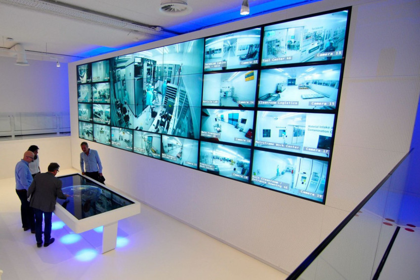
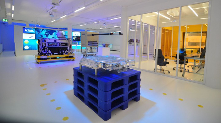
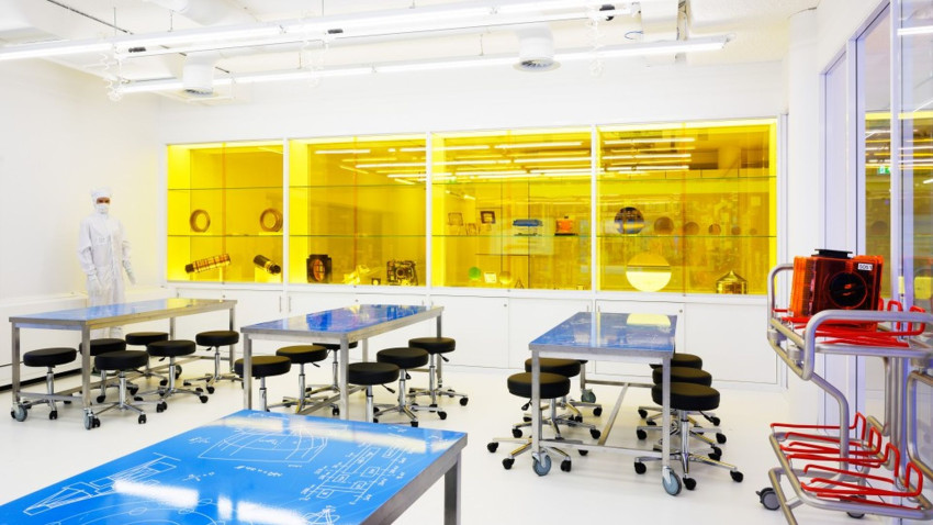
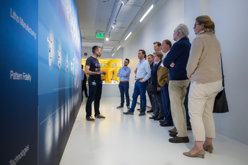
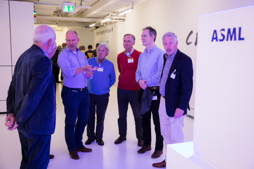
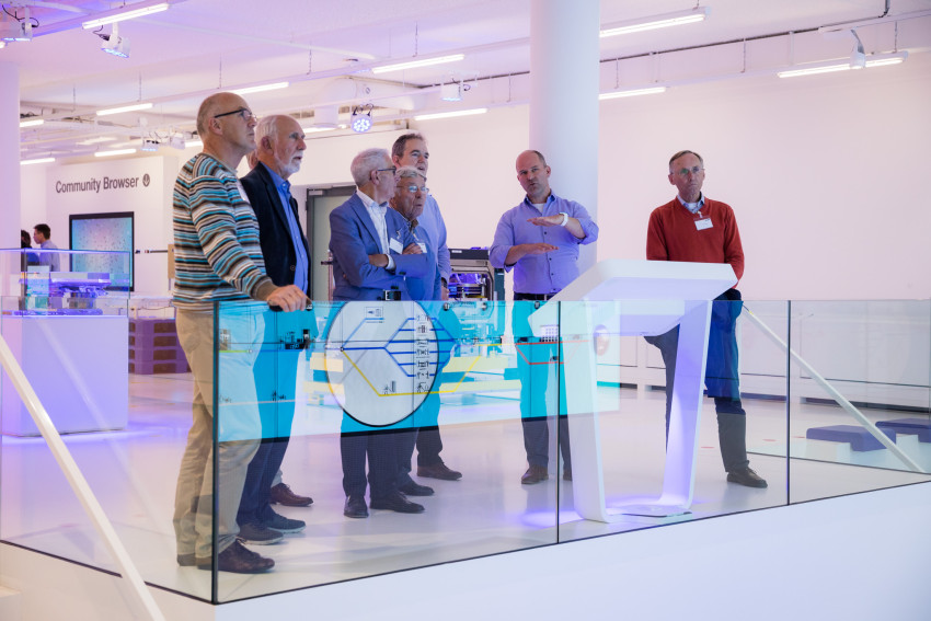
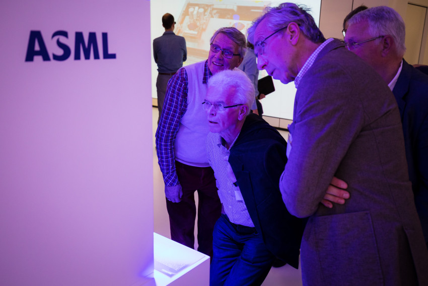
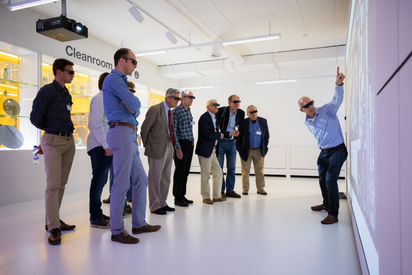
A general impression of ASML technology and systems will be given during a tour of the experience center. Special attention for the role of new, young employees (Young ASML) from all over the world.
Registration
KIVI-E members, Young KIVI members and KIVI students can register straight away and will receive a valid confirmation e-mail. Bring this printed e-mail with you for register at the reception.
Others will be put on a reserve list. Later a mail will be send to inform you about acceptance or rejection of your participation request.
In case the event is fully booked and you would like to be on the reserve list please let the KIVI-organizer know by sending a mail.
Spreker(s)
Ir. Maarten Hoeks, Manager Electrical Architecture Group at ASML
Ir. Jeroen van Duivenbode, Competence Leader Power and High Voltage Electronics at ASML and TU/e Fellow at Department of Electrical Engineering at TU/e.
Locatie
ASML Netherlands B.V. Building 7 Reception
The Run 6665, 5504 DR Veldhoven
Organisator
Elektrotechniek
ASML Netherlands B.V.
Naam en contactgegevens voor informatie
ir. Steven Luitjens 06 46 72 66 89
